|
The activities concerning this technological area are focused on using microelectronic technologies for the study and realization of materials, devices and systems for photonic and optoelectronic applications in areas related to biomedicine, ICT, aerospace and environment.
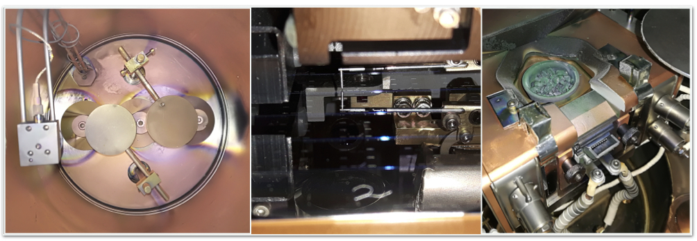
Main activities carried out in the Clean Room facility at the IMM - Unit of Napoli, are:
- Fabrication of optoelectronic devices, both active and passive, like photodetectors, waveguides, optical sensors, or planar optical structures like Bragg reflector, high and low reflectivity optical coating, a-periodic structures, etc. The fabrication processes needed for this kind of applications involve many technologies, like e-beam and photo lithography, thin film deposition, dry and wet etching and metal deposition.
- Fabrication of plasmonic and dielectric metasurfaces devices directly on the optical fiber tip. The fabrication process essentially consists of three main technological steps: spin coating deposition of electron-beam resist with accurate thickness control and flat surface over the fiber core region; e-beam exposure and development.
- Fabrication of micro-fluidic devices in poly(dimethylsiloxane) (PDMS) by soft lithography technique. This process is based on the rapid prototyping and replica molding using the PDMS, an elastomeric material. The procedure consists in the fabrication of the master by photolithographic processes, using SU-8 photoresist, the replica molding by casting the PDMS against the master and sealing of the micro-fluidic system through bonding to a flat surface by a O2 plasma
These activities are fully integrated in the chain design-fabrication-characterization that distinguishes the IMM - Unit of Napoli, allowing the manufacturing at home what is being designed within the Modeling Area, and then characterized in the Characterization Area.
Coordinator: Gioffrè Mariano
|